![]()
![]()
The research focus of our group “Nanostructuring and Scanning Probe
Techniques” (www.schimmel-group.de)
is on fabrication, analysis, properties and applications of functional
nanostructures. We develop the corresponding techniques for nanolithography
(“Top-Down Approach”) as well as novel processes for nanostructure
formation by self-organization (“Bottom-Up Approach”). The
Atomic Force Microscope (AFM) is used both for structuring and imaging.
The developments of our group, which lead to 20 patents filed so far, include
the world´s smallest transistor, a novel process allowing for nanocontact
printing and crystalline nanowires with 30-fold increased mechanical yield
strength.
 Atomic-Scale
Electronics – Switching Quantum Currents with Individual Atoms
Atomic-Scale
Electronics – Switching Quantum Currents with Individual AtomsThomas Schimmel and Fangqing Xie
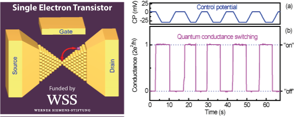
The Atomic Transistor. The controlled repositioning of
one single silver atom allows for the reversible opening and closing of an
electronic circuit.
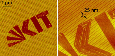 Nanoanalytics and Nanolithography with Scanning Probe Techniques
Nanoanalytics and nanolithography via AFM. Functional chemical
patterns on surfaces can be written and subsequently imaged with the same AFM
tip.
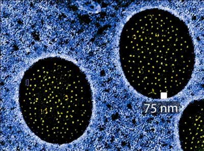 (Bio)functional and Biomimetic Nanostructured Surfaces
Pattern formation of the nanometer scale by self-organization.
An example for biofunctional films is shown.
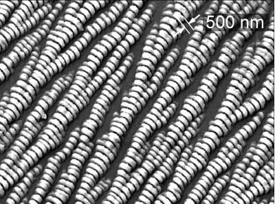 Pattern Formation and Self-Organization
on the Nanometer Scale
Pattern Formation and Self-Organization
on the Nanometer ScalePattern formation of the nanometer scale by self-organization.
An example is shown for metallic nanowires.